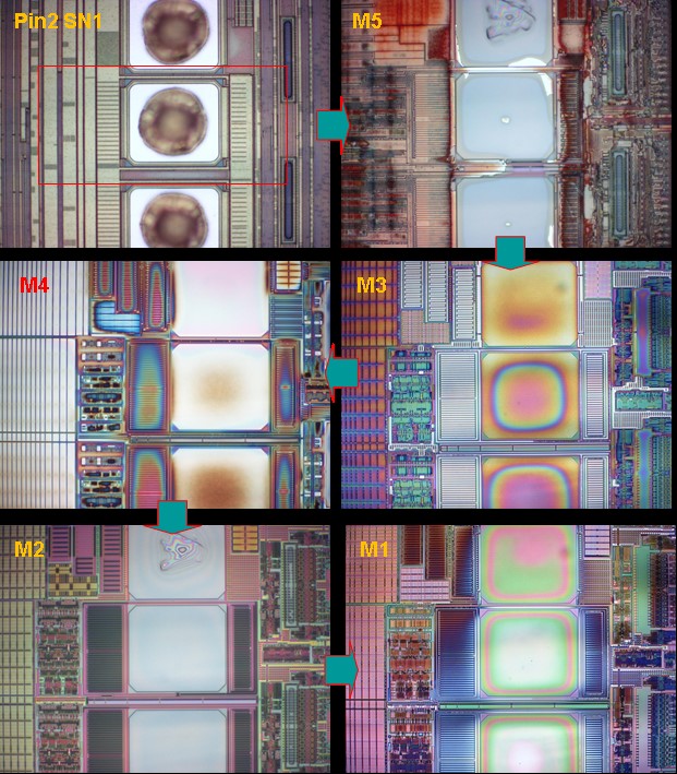
This destructive process consists of removing each layer of die to expose for inspection and further analysis. The process uses chemical solution/gas etching and mechanical polishing to slowly and precisely remove each layer of the die. Typical die layers consist of plasma, oxide, and metal. Planarity is critical in deprocessing applications where individual device layers are sub microns.
The most common application of parallel lapping is for I.C. delayering, but it can also be used to thin PCBs, compound semiconductors, and a variety of other materials.
