AFM Analysis
AFM Force Curve Analysis | AFM Image Analysis | AFM Surface Analysis | AFM Roughness Analysis
Atomic Force Microscopy (AFM)
Atomic Force Microscopy (AFM) or Scanning Probe Microscopy analysis uses a tip that is attached to a cantilever that moves over the specimen surface to generate images with a near-atomic resolution for measuring surface topography. The tip is scanned laterally and the force between the tip and the sample is measured and recorded to generate the topography of the surface. There are a few modes of measurements as follows:
- Very flat surface – In this mode, one edge of the cantilever is kept fixed and the other edge with the tip is moved vertically; as it moves over the surface the data is recorded to generate the topographic image.
- Oscillation mode – In this mode, the cantilever oscillates near its resonate frequency, while the oscillation amplitude is recorded. A stiff cantilever is oscillated in the interested region, meaning that the tip is quite close to the specimen, but not touching the sample. The measurement scheme is based on measuring changes to the resonant frequency or amplitude of the cantilever as the interaction between the tip and sample dampens the oscillation.
- In all modes, a laser attached to the tip of the cantilever measures the position of the tip with respect to the surface.
- AFM is capable of quantifying the surface roughness of samples down to the angstrom scale. In addition to presenting a surface image, AFM analysis can also provide quantitative measurements of feature sizes, such as step heights and other dimensions.
Where do we use AFM?
- Generate topography images
- Nano electrical characterization
- Material properties
- Friction
- Electrical forces
- Capacitance
- Magnetic forces
- Conductivity
- Viscoelasticity
- Surface potential
- Resistance
AFM is widely used in failure analysis and wafer processing of ICs. AFM is used in IC’s Redistribution Layer (RDL), Chemical Mechanical Polishing (CMP), and Under Bump Metallization (UBM) process now. Research is focused on measuring and monitoring differences between pre-and post-etching as any abnormal roughness is very likely to result in a loss of coated film and even reliability issues.


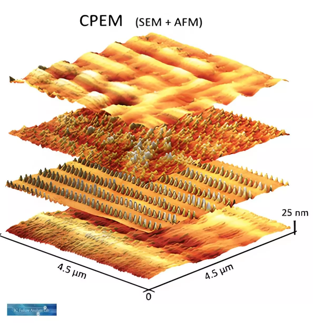
What is the difference between SEM and AFM?
The SEM gives magnification in two dimensions: X and Y. The AFM gives magnification in three dimensions: X, Y, and Z… AFMs also provide different magnifications in the X, Y, and Z axes. While SEMs scan a sample surface much faster than an AFM, they are not actually faster to use than an AFM scanning.
Conclusion
AFM is a powerful tool used in failure analysis of semiconductor devices as well as inspection of surface roughness, and contamination in chip foundries.
optical microscopy failure analysis • Counterfeit Component Authenticity • Cross Section Analysis • Parallel Lapping • Energy Dispersive X-Ray Spectroscopy • Focused Ion Beam • i-v curve analysis • Photoemission microscopy failure analysis • Scanning Acoustic Microscopy • electron microscope services • Secondary Ion Mass Spectrometry • IC X-Ray services