Photoemission microscopy failure analysis
Photo Emission Microscopy
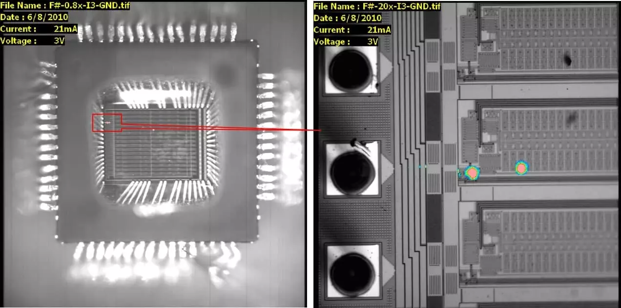
Photoemission or light emission microscopy, e.g., Hot Spot Inspection, is an advanced failure analysis technique for detecting photonic radiation from a defective site due to excessive heat generated at the defective site. The emission light is not visible to the naked eye.
Photoemission microscopy uses powerful imaging equipment to intensify low-emitted lights that can be visible through a CCD camera. The emitted light location coincides with the precise location of the defect on the die surface image. The following are three different techniques used in this analysis:
EMMI (Emission Microscopy) :
EMMI is non-invasive and can be performed from either the back or front of the specimen. The sample is electrically powered and compared to a known good device under the emission microscope. Emitted photons are detected by a highly-sensitive CCD camera. EMMI is capable of detecting light wavelengths between 350 nm and 1100 nm. EMMI is used for detecting leakage current resulting from device defects, e.g., Gate oxide defects / Leakage, Latch-Up, ESD Failure, junction Leakage, etc.
InGaAs EMMI (Indium Gallium Arsenide Emission Microscopy) :
InGaAs EMMI is similar to the EMMI technique. However, InGaAs EMMI uses InAgAs detectors for the detection of emitted photons at the defect site. This technique shifts the detection of InGaAs to a longer wavelength range, between 900 and 1700 nm (infrared). InGaAs EMMI is 5 to 10 times faster and is more sensitive than EMMI.
OBIRCH (Optical Beam Induced Resistance Change) :
Optical Beam Induced Resistance Change (OBIRCH) is used in semiconductor failure analysis to detect and localize electrical defects in integrated circuits (ICs) or chips. It is particularly effective in identifying open or short circuits in ICs, which can cause device malfunctions.
OBIRCH works by illuminating a specific area of the IC with an infrared laser beam. When the laser interacts with the IC, it generates heat. This localized heating causes the resistance of the electrical path in that area to change. It is possible to detect and locate defects by measuring the resistance change.
The OBIRCH technique is based on the principle that the electrical resistance of a circuit is affected by the local temperature. When a defect such as an open or short circuit is present, it can cause localized heating due to increased current flow or resistive heating. This heating changes the electrical resistance in the affected area, which can be detected and measured using OBIRCH.
A focused laser beam is directed onto the IC under test to perform OBIRCH analysis. The laser spot size is typically a few micrometers, allowing for high-resolution defect localization. The resistance change is monitored by measuring the voltage drop across the region of interest or observing the current flowing through the circuit.
OBIRCH is a non-destructive analysis technique that does not damage the IC during testing. It is commonly used in semiconductor manufacturing and failure analysis laboratories to identify and troubleshoot defects in ICs. By pinpointing the location of electrical failures, engineers can perform targeted repairs or design improvements to enhance the reliability and performance of integrated circuits.

i-v curve analysis • ic decapsulation service • Counterfeit Component Authenticity • Cross Section Analysis • Parallel Lapping • Energy Dispersive X-Ray Spectroscopy • Focused Ion Beam • optical microscopy failure analysis • Scanning Acoustic Microscopy • electron microscope services • Secondary Ion Mass Spectrometry • IC X-Ray services