X ray inspection systems are key tools for failure analysis, quality control, and yield enhancement of Integrated Circuits (ICs), active & passive components, and Printed Circuit Boards (PCBs). In many cases, IC X-Ray Services (2D and 3D) provides the only non-destructive techniques to inspect optically hidden components and solder joints such as BGA, POP, QFN, flip chips, through holes, TSVs, micro-bumps, copper pillars, etc. There have been significant improvements in the X-ray inspection capabilities (both 2D and 3D) in the last several years.
While contrast imaging is a very powerful and widely used technique, there is significantly more information present within the X ray beam, which, until now, has not been exploited in electronics inspection. Instead of simply measuring the total absorption of the X ray beam, a physical structure known as a Multi Absorption Plate (MAP) can be placed in the beam path. This, coupled with machine learning algorithms, enables material type and thickness information to be acquired alongside the standard grey-scale image.
IC Failure Analysis Lab uses the state-of-the-art 2D and 3D X-Ray machines to meet today’s non-destructive inspection of electronic components and provide clear and high quality digital images of the samples with fast turn around and lower costs. You can request a free quote for IC X-Ray Services right now.
3-D X-Ray / Computed Tomography (CT) X-Ray
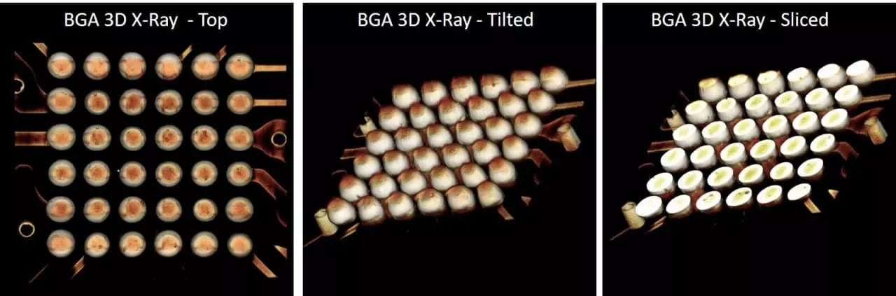
3D X-ray or CT X-Ray is a real time completely non-destructive and non-contact failure analysis technique that allows you to view and inspect the external and internal construction of a sample in 3D space. 3D X-Ray works by taking hundreds or thousands of 2D X-Ray images around a 360° rotation on a sample. The proprietary state of art algorithm takes these 2D X-ray images to reconstruct them into a 3D CT volume image. The 3D CT volume image will allow you to view, measure and slice the part at any angle.
3D CT practically eliminates interpretation errors and opens the door to many capabilities; some not available with any other technology
2-D X-Ray
2D X-ray is a non-destructive failure analysis technique to inspect internal construction of a sample. An X-Ray inspection is used to identify damaged, broken, shorted… interior of semiconductors. Comparative X-Ray images from a failing device and a reference sample are fast and low cost inspection methods that are used in design, development, production and fault isolation of semiconductors.
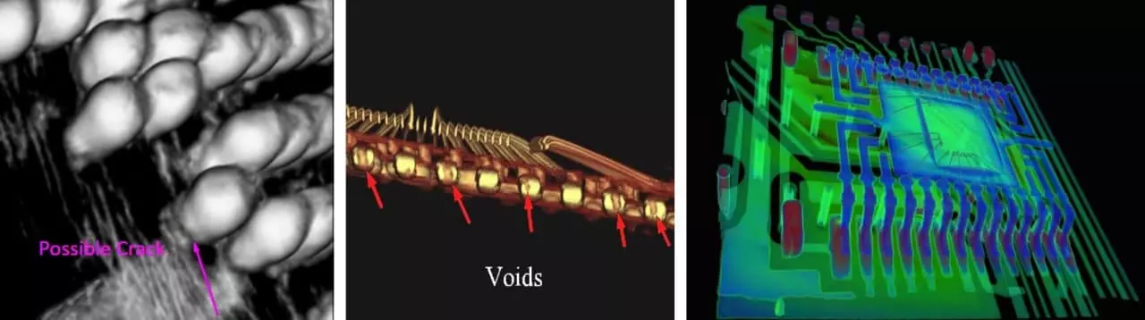
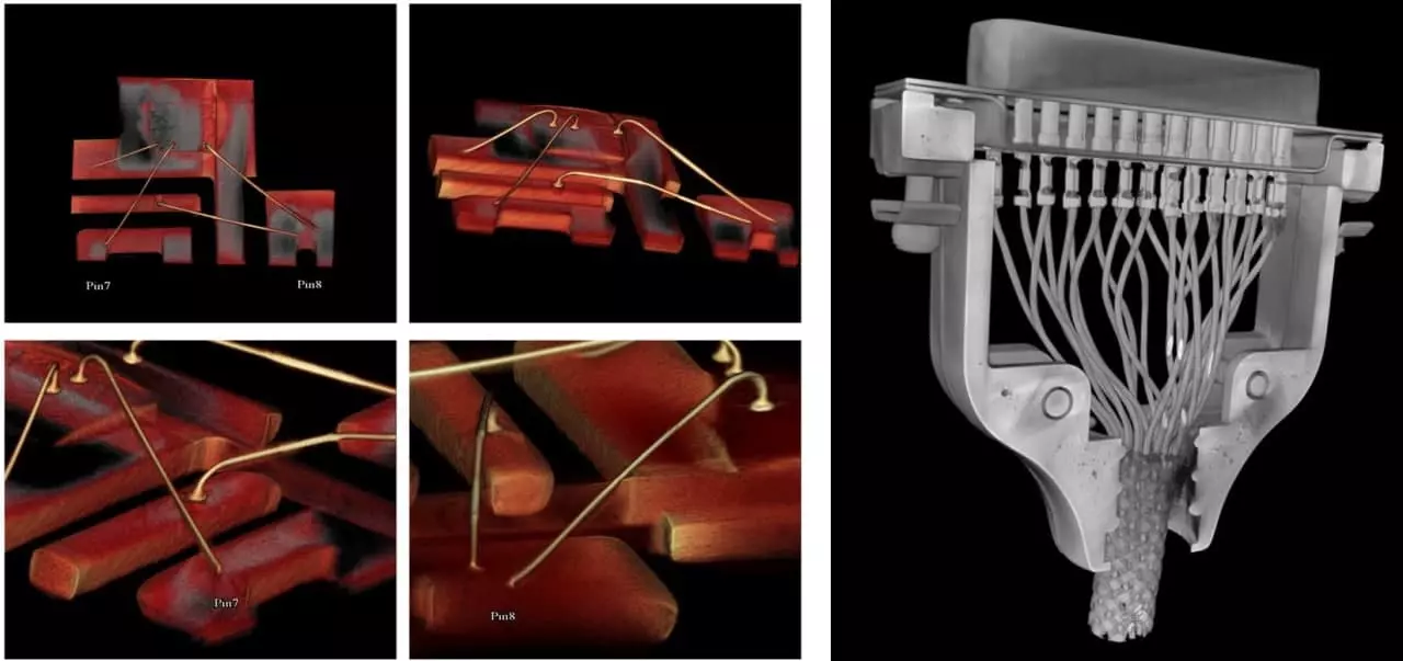
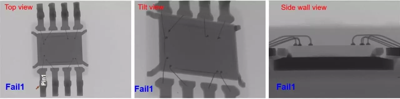
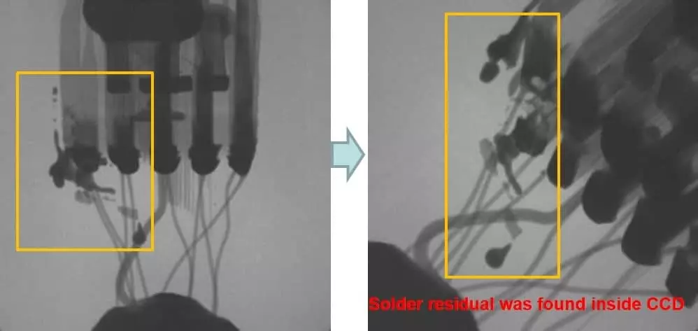
X-ray images can reveal cracks, wire bonds anomaly, die size, voids… in an electronic device. The following are a few pictures of 2D X-Rays.
